Indonesia Semiconductor & Optical Sourcing White Paper
Top 10 Quartz Wafer Manufacturer & Exporter for the Indonesia Market
A comprehensive engineering benchmark on fused silica substrates, high-purity optical flats, and high-temperature thermal quartz processing solutions aligned with Making Indonesia 4.0 industrial acceleration.
Precision Thermal & Substrate Tooling
Essential Quartz & Infrared Process Solutions for Indonesian Facilities
Engineered for photovoltaic manufacturing, thin-film annealing, rapid thermal processing (RTP), PET industrial blow moulding, and laboratory biochemical diagnostics across Greater Jakarta, Surabaya, and Batam industrial corridors.
The Strategic Role of Quartz Wafers and Fused Silica in Indonesia's Industrial Transformation
As the Republic of Indonesia advances its ambitious economic master plan under the "Making Indonesia 4.0" blueprint and deepens industrial downstream processing (Hilirisasi), the domestic consumption of microelectronics substrates, semiconductor-grade quartzware, and precision optical flats has entered an unprecedented growth phase. Industrial development initiatives across the Batam Free Trade Zone (FTZ), the Cikarang-Karawang industrial corridor in West Java, and the newly established Kendal Industrial Park in Central Java have triggered a significant shift toward local electronic assembly, solar photovoltaic cell lamination, and precision optical component manufacturing.
In these advanced fabrication regimes, the quartz wafer (fused silica substrate) functions as an indispensable core element. Unlike conventional borosilicate or sodalime glass, high-purity fused quartz (SiO2 ≥ 99.99%) possesses an exceptionally low coefficient of thermal expansion (approx. 5.5 × 10⁻⁷ / K between 20°C and 320°C), an ultra-wide optical transmission spectrum spanning deep ultraviolet (DUV 190 nm) to the near-infrared (NIR > 2500 nm), and supreme dielectric strength. These distinct physical traits make quartz wafers the material of choice for photolithography mask blanks, MEMS (Micro-Electro-Mechanical Systems) pressure sensors, high-frequency telecommunication SAW filters, and high-temperature thermal carriers used in semiconductor diffusion furnaces.
Top 10 Quartz Wafer Manufacturers and Global Exporters Serving Indonesia
For Indonesian procurement officers, cleanroom facility managers, and research institutions such as BRIN (Badan Riset dan Inovasi Nasional), identifying dependable international manufacturers requires a rigorous evaluation of raw material pedigree, double-sided polishing capabilities, Total Thickness Variation (TTV) control, cleanroom packaging standards, and direct trade logistics. Below is the authoritative industry analysis of the top 10 global quartz wafer manufacturers and exporters actively fulfilling supply chain requirements for the Indonesian archipelago:
1. Kavri Quartz Product Co., Ltd.
Direct OEM / Cost Leader
Headquartered in Lianyungang, Jiangsu—the premier raw quartz processing cluster in China—Kavri Quartz provides factory-direct custom quartz wafers, polished fused silica flats, and complementary quartz diffusion tubes. Specializing in rapid prototyping, low-MOQ orders (from 10 pcs), and OEM dimension customization from 1-inch to 12-inch wafers with Ra < 0.5 nm finish.
Key Advantage: Direct mine-to-finished substrate supply chain control
Delivery Speed: Air express DDP direct to Jakarta, Batam, & Surabaya
2. Heraeus Conamic
Global Pure-Play Silica
A German multinational technology giant renowned for high-purity synthetic fused silica grades (Suprasil®). Heraeus delivers semiconductor-grade ingots and polished wafers primarily catering to tier-one microchip foundries and specialized DUV optics installations across Asia.
Key Advantage: Near-zero internal bubble and inclusion levels
Target Segment: High-budget microelectronics and laser laboratories
3. Shin-Etsu Chemical Co., Ltd.
Semiconductor Tier 1
Based in Japan, Shin-Etsu is an undisputed benchmark in semiconductor silicon and synthetic quartz substrates. They supply ultra-flat wafer substrates for extreme ultraviolet (EUV) and photolithography mask blanks with rigorous wafer-to-wafer uniformity standards.
Market Profile: Long contract cycles for high-volume device producers
4. Tosoh Corporation
Material Specialist
Tosoh Quartz designs advanced silica glass fabrication solutions for dry etching, diffusion, and oxidation systems. Their quartz substrate plates and wafers exhibit premier resistance against plasma erosion in corrosive semiconductor atmospheres.
Distribution: Channel partners throughout Singapore and Southeast Asia
5. Corning Incorporated
Specialty Glass Leader
Originating in the USA, Corning provides HPFS® (High Purity Fused Silica) wafers designed for exceptional optical homogeneity and high laser-induced damage thresholds (LIDT). Highly favored for precision sensor and aerospace applications in Southeast Asia.
Key Advantage: Low birefringence and high refractive index uniformity
Application: Deep UV optical windows and interferometer optics
6. CoorsTek, Inc.
Technical Ceramics & Quartz
CoorsTek brings decades of material expertise in advanced ceramics and fused quartz components for semiconductor equipment. They provide high-durability quartz carrier disks, boat assemblies, and inspection wafers to testing plants in the ASEAN region.
Key Advantage: Robust mechanical tolerance and high structural yield
Support: Engineering offices in Singapore serving Indonesian clients
7. Edmund Optics
Optical Catalog Pioneer
A premier international distributor and optical fabrication supplier providing pre-cut fused quartz and fused silica transmission windows, test wafers, and optical flats. A standard resource for Indonesian universities and prototyping laboratories.
Key Advantage: Small-batch stock availability with short delivery times
Limitation: Higher unit cost for high-volume custom production
8. Technical Glass Products (TGP)
Custom Fabricator
Based in North America, TGP specializes in precision CNC machining, custom flame-working, and polishing of fused quartz and fused silica products, including wafer boats, crucibles, and customized round wafer discs.
Key Advantage: Tailored dimensional cut-outs, notches, and flats
Market: Specialized tool builders and research reactors
9. Swift Glass Company
Precision Glass Processor
An established American glass fabrication specialist possessing waterjet cutting, lapping, and polishing certifications for specialized industrial windows, sight glasses, and fused silica wafer substrates.
Key Advantage: High-yield edge chamfering and beveling technology
Logistics: Experienced with international export compliance
10. UQG Optics
European Optical Flats
Located in the United Kingdom, UQG Optics supplies commercial and optical-grade fused quartz plates, discs, and wafers. They cater extensively to scientific instrumentation builders and biomedical diagnostic apparatus assemblers across Southeast Asia.
Key Advantage: Strict surface flatness testing (up to λ/10 per inch)
Focus: UV spectrometry substrates and biochemical cell bases
When procuring quartz wafers for deployment in Indonesian industrial environments, choosing the correct material grade directly determines yield rates, thermal survivability, and spectral transmission. Below is a detailed engineering reference comparing the standard grades of quartz wafers provided by Kavri Quartz and leading global exporters:
Wafer Grade Category
Raw Material Purity (SiO2)
Surface Roughness (Ra)
TTV & Flatness Tolerance
Dominant Transmission Band
Typical Industrial Deployment
Semiconductor Prime Grade
≥ 99.999% (< 0.1 ppm Fe, Al, Ti)
≤ 0.3 nm – 0.5 nm (CMP Polish)
TTV < 2 µm, Bow/Warp < 10 µm
DUV & Visible (200 nm – 2000 nm)
IC Photolithography masks, Thin-film epitaxy, Sub-micron MEMS
Infrared pyrometry windows, Thermal imaging sensors, IR emitters
Localized Application Scenarios in the Indonesian Archipelago
The operating conditions within Indonesian factories require specific adaptations due to the equatorial tropical climate (high ambient humidity > 80% and temperatures hovering around 32°C) alongside the targeted industrial focuses of each regional manufacturing hub. Here is how precision quartz wafers and specialized infrared thermal components intersect with local production demands:
Solar PV Cell Fabrication & Stringer Soldering
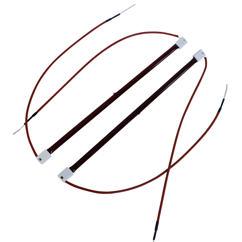
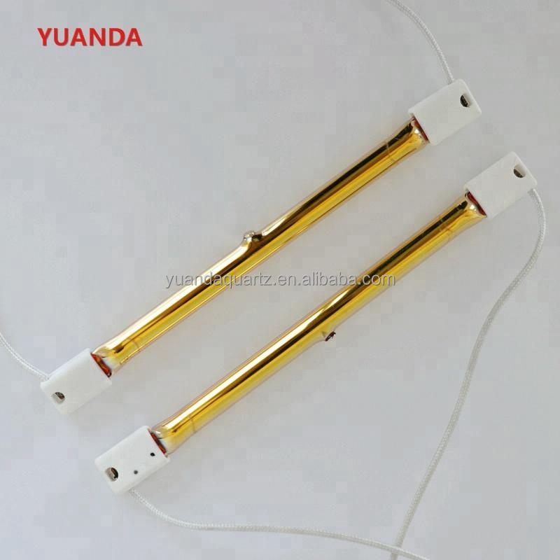
Under Indonesia's National Energy General Plan (RUEN), solar farm installations are booming in West Java, Riau, and East Nusa Tenggara. Quartz wafers and high-purity clear fused quartz tubes serve as thermal susceptors and isolation shields in silicon wafer diffusion, while our 120V/220V infrared emitters achieve high-speed, contactless stringer soldering without micro-cracking thin silicon cells.
Batam FTZ Electronics & Micro-Sensors (MEMS)
Operating within bonded zones such as Batamindo Industrial Park, multinational electronics producers manufacture precision sensors, telecommunications filters, and optoelectronic modules. Polished 4-inch and 6-inch quartz wafers are used as electrical insulating substrates due to their minimal dielectric loss tangent (< 0.0001 at 10 GHz) and superior optical clarity.
Biomedical Diagnostic Apparatus & Clinical Labs
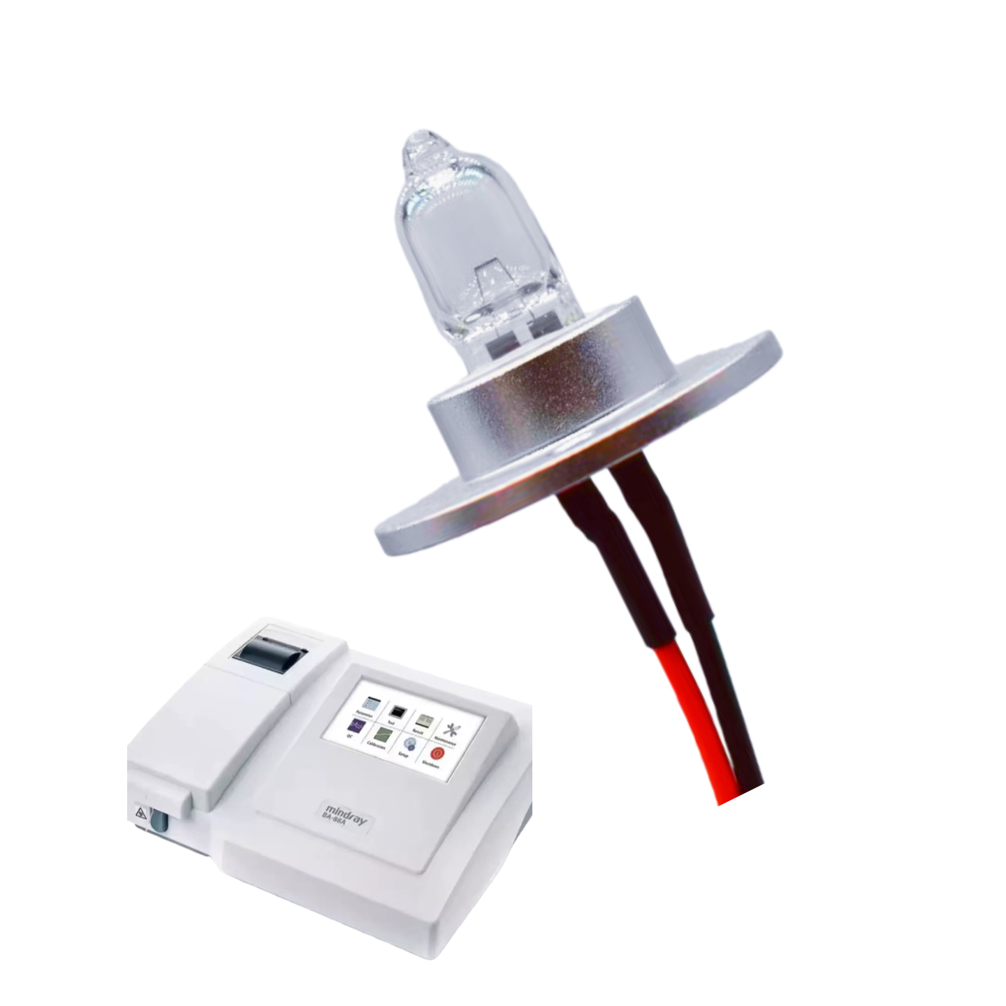
With national healthcare infrastructure expanding across Jakarta and regional hubs, diagnostic instrument manufacturers rely on optical quartz micro-flow cells and precision analyzer bulbs (such as the BA-88A halogen light sources) to deliver uncompromised spectral accuracy for blood serum spectrometry and enzymatic testing without UV absorbance distortion.
Analyzing the macroeconomic trajectory through 2026–2030 highlights three transformative trends directly impacting quartz wafer and thermal emitter consumption in Indonesia:
Localized Solar Supply Chain Mandates (TKDN Compliance): The Ministry of Industry (Kemenperin) has established stricter Domestic Component Level (TKDN) regulations for renewable infrastructure. To satisfy these thresholds, solar module assemblers are investing heavily in domestic wafer lamination, cell testing, and rapid thermal processing equipment that require premium quartz heating envelopes and alignment wafers.
Accelerated EV Ecosystem & Battery Power Electronics: The establishment of battery cell giga-factories in Karawang and Morowali creates massive downstream demand for power semiconductors (MOSFETs, IGBTs). Silicon-on-insulator (SOI) and quartz carrier substrates are vital in prototyping these wide-bandgap components under high continuous thermal stresses.
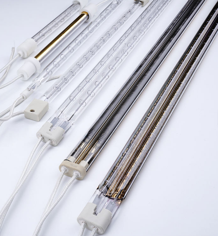
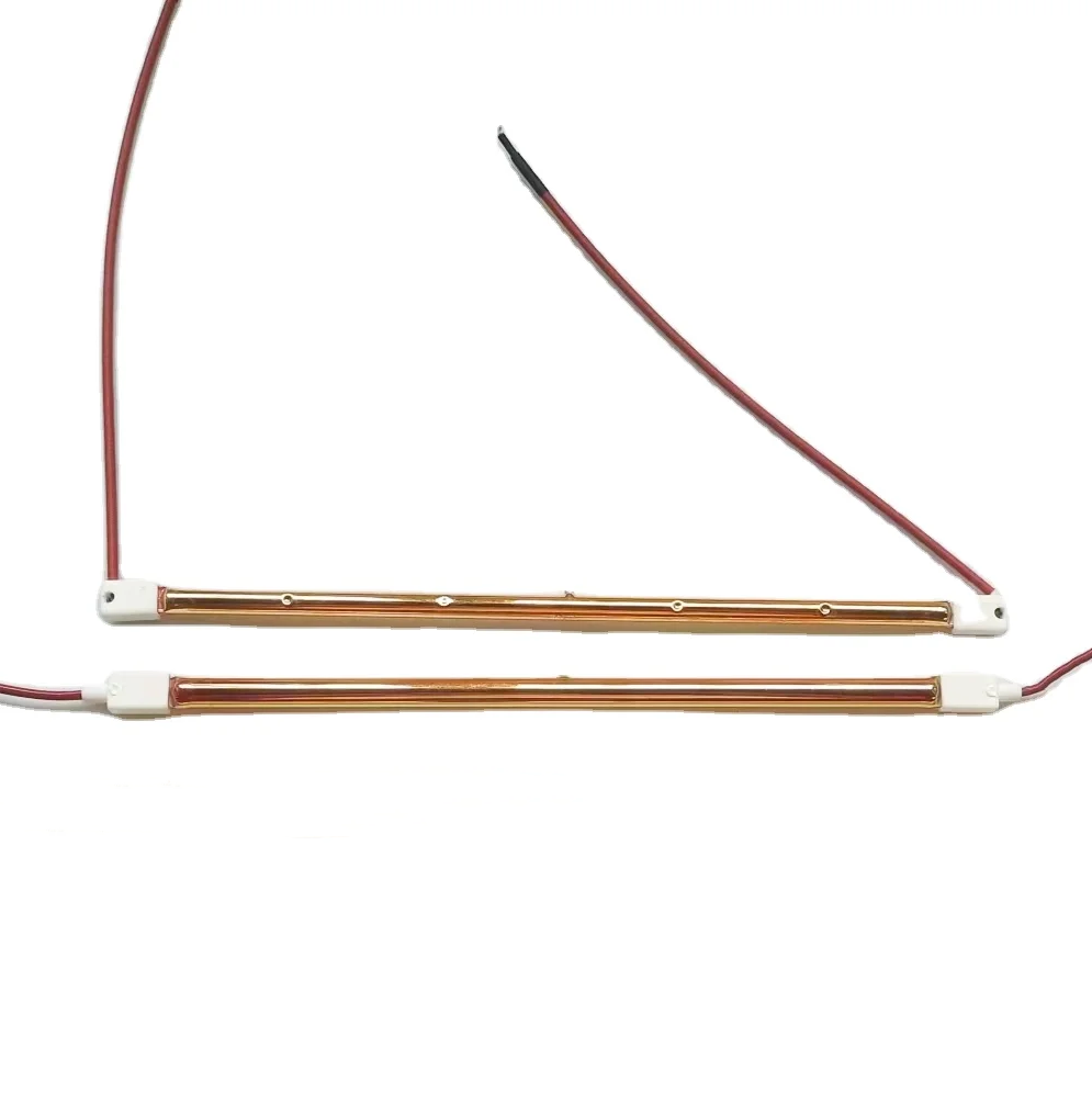
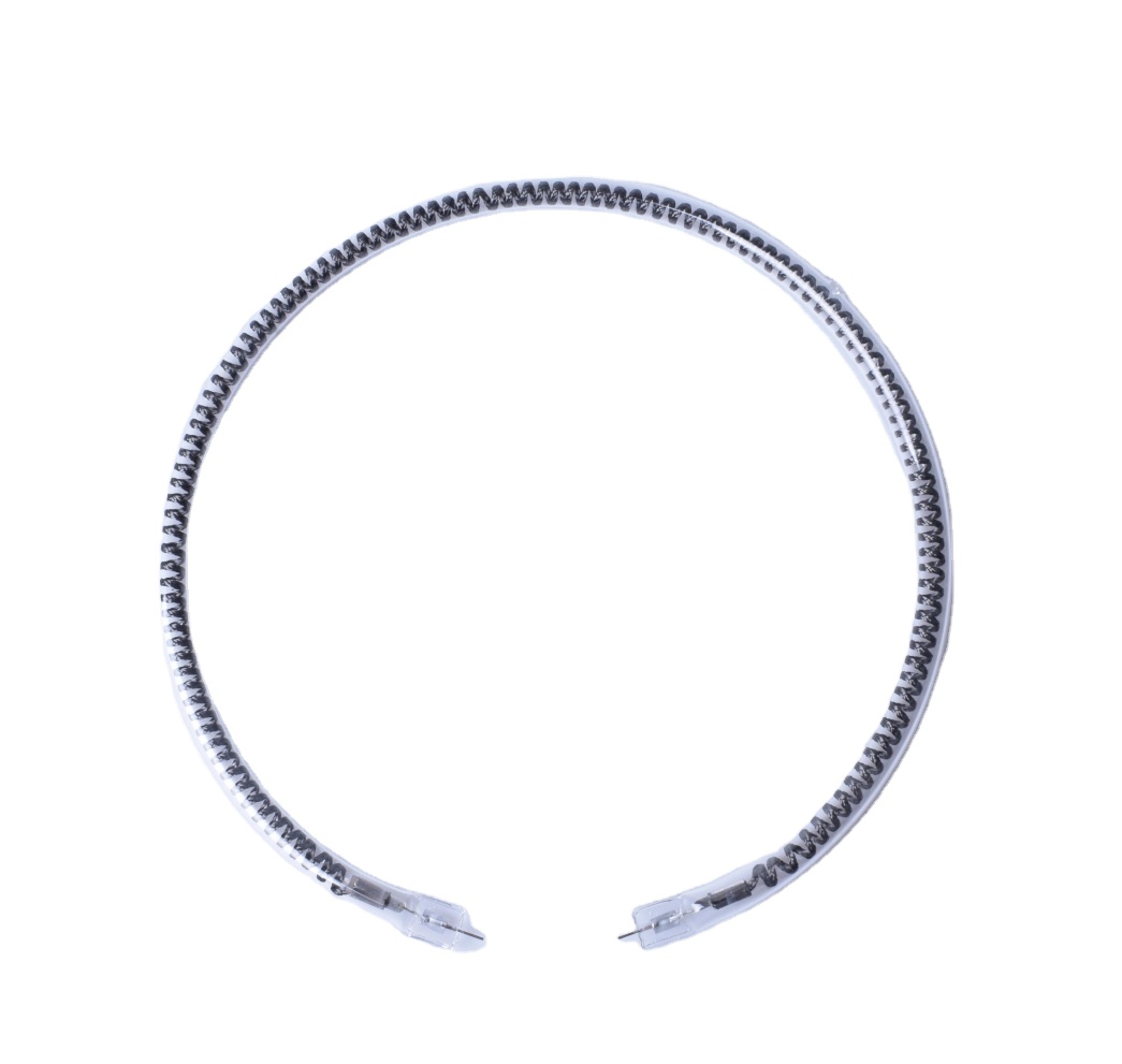
Energy-Efficiency Retrofits in High-Speed Packaging: Food and beverage conglomerates operating in Bekasi, Surabaya, and Medan are aggressively transitioning away from bulky convective ceramic heating toward short-wave halogen infrared quartz emitters. This transition cuts electrical energy consumption by up to 38% in PET bottle blow moulding while eliminating line downtime.
Factory-Direct Authority
Why Indonesian Enterprises Partner with Kavri Quartz
Direct access to China's leading quartz production cluster with verified quality management, rapid engineering cycles, and end-to-end export compliance.
Geographic Raw Silica Superiority
Situated in Niushan Street, Donghai / Lianyungang, we operate at the epicenter of high-purity natural silica refining, guaranteeing 99.99% SiO2 baseline raw purity with zero batch contamination.
10+ Years OEM / ODM Experience
Founded in 2014 with 3 dedicated production lines, we fabricate custom wafer diameters, thicknesses, notch alignments, and infrared emitter assemblies strictly according to client CAD drawings.
Agile Quoting ≤ 4-Hour Response
Our dedicated bilingual engineering export team operates with an average response time under 4 hours, providing rapid technical drawings, custom prototyping, and verified inspection test reports.
81%–90% Global Export Volume
Trusted across Germany, the Netherlands, Japan, South Korea, and Southeast Asia. We maintain long-term partnerships with leading machine manufacturers and testing facilities worldwide.
Zero-Damage Tropicalized Packaging
All quartz wafers and lamps are packed using vacuum nitrogen-flushed conductive trays, multi-layer closed-cell foam shock absorbs, and fumigated timber crates proven against high ocean humidity.
Direct Freight to Tanjung Priok & Batam
Supporting EXW, FOB, CFR, CIF, and full DDP terms with transparent customs documentation (Form E, Certificate of Origin) to facilitate zero-tariff import under the ACFTA agreement.
Procurement Guidance
Frequently Asked Questions by Indonesian B2B Buyers
Clear answers regarding import compliance, customs clearance at Indonesian seaports, minimum order quantities, and technical validation.
What are the customs clearance requirements for importing quartz wafers and infrared lamps into Indonesia?
Importing into major ports such as Tanjung Priok (Jakarta), Tanjung Perak (Surabaya), or Batu Ampar (Batam FTZ) requires standard documentation: Commercial Invoice, Packing List, Bill of Lading (B/L), and an active NIB (Nomor Induk Berusaha). Furthermore, by utilizing our Form E (ASEAN-China Free Trade Area) certificate, Indonesian importers can typically secure preferential or zero-rate import duty on industrial quartz and fused silica glass products under HS Codes 7002.31 and 7002.39.
How do you protect fragile quartz wafers and glass emitters from tropical moisture during ocean freight?
Given Indonesia's equatorial transit conditions, moisture ingress can cause surface condensation stains or dielectric degradation. We package optical quartz wafers inside cleanroom-grade antistatic fluoroware wafer cassettes, sealed within vacuum-evacuated aluminum foil barrier bags containing high-capacity silica gel desiccants. Infrared lamps and long quartz tubes receive individual polyethylene sleeving, surrounded by customized high-density shock-absorbing EPE foam within reinforced fumigated wooden cases engineered to withstand maritime humidity and transit vibration.
What is the Minimum Order Quantity (MOQ) for custom-dimension quartz wafers?
To support both academic prototyping (e.g., UI, ITB, BRIN research) and pilot production runs, our standard MOQ for custom polished quartz wafers (from 2-inch to 8-inch diameters) starts at just 10 pieces. For standard catalogue infrared heating lamps and quartz tubes, trial batches begin from 8 to 10 units. High-volume repeat container shipments benefit from scaled volume discounts.
Can you replicate or customize infrared heating elements for older European or Japanese equipment?
Yes. With more than 10 years of specialized OEM reverse engineering experience, we routinely build precise drop-in replacements for aging Japanese, German, and Italian manufacturing lines. If an original manufacturer's blueprint is unavailable, you only need to provide the tube profile (single or twin tube), overall length, heated length, voltage, wattage, end ceramic cap profile, and a photo of the original lamp's markings. Our engineering department can calculate filament resistance and deliver sample units within 7 working days.
How does fused quartz compare against borosilicate glass for high-temperature Indonesian factories?
Borosilicate glass (such as Pyrex) has an operating limit around 450°C to 500°C and a thermal expansion coefficient around 32.5 × 10⁻⁷ / K. In contrast, fused silica quartz withstands continuous operating temperatures up to 1,100°C (with short-term peak exposures reaching 1,450°C) and features a thermal expansion rate almost six times lower (5.5 × 10⁻⁷ / K). This allows a red-hot quartz wafer or tube to be plunged directly into cold water without shattering, making it essential for rapid thermal processing (RTP) and plasma etch chambers.
What quality control documentation is supplied with each quartz wafer order?
Every production batch leaves our facility with a comprehensive Certificate of Analysis (COA) detailing: Spectrographic chemical purity analysis, surface roughness (Ra) profilometer reports, interferometric flatness data (TTV, Bow, Warp), dimensional tolerance verification, and high-voltage dielectric insulation test passes. Pre-shipment video verification is also standard for all direct export orders to Indonesian ports.
Accelerate Your Precision Thermal & Substrate Supply Chain
Whether you require prime-grade polished quartz wafers for cleanroom microfabrication or custom-wattage infrared emitters for automated production lines in Indonesia, our engineering specialists provide detailed quotations and technical reviews within 4 hours.