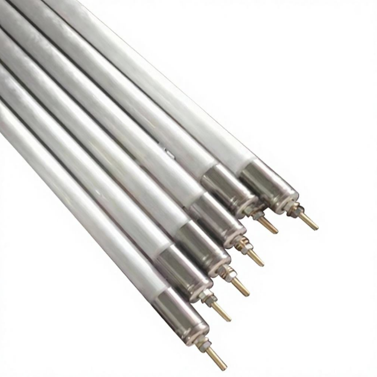
Electric Furnace Wire Quartz 1000W for Equipment
- Nichrome / FeCrAl internal core
- High thermal shock resilience
Direct from our Lianyungang processing center to San Jose and the wider Bay Area: High-purity resistance elements, optical emitters, and ceramic interfaces manufactured under strict international tolerances.
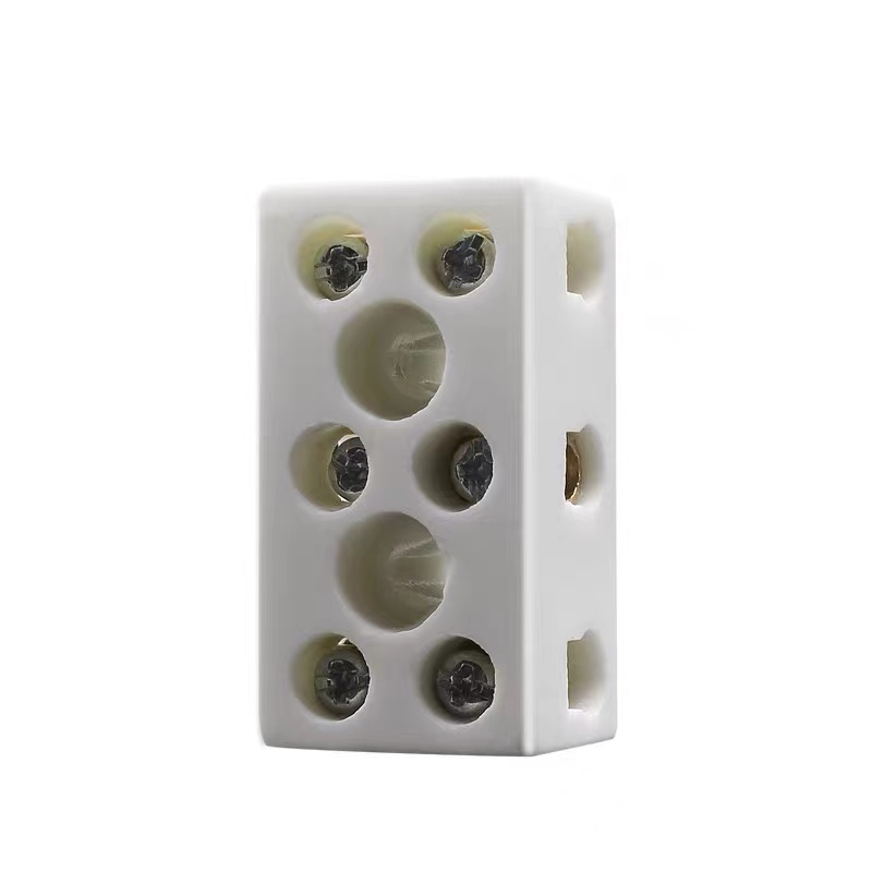
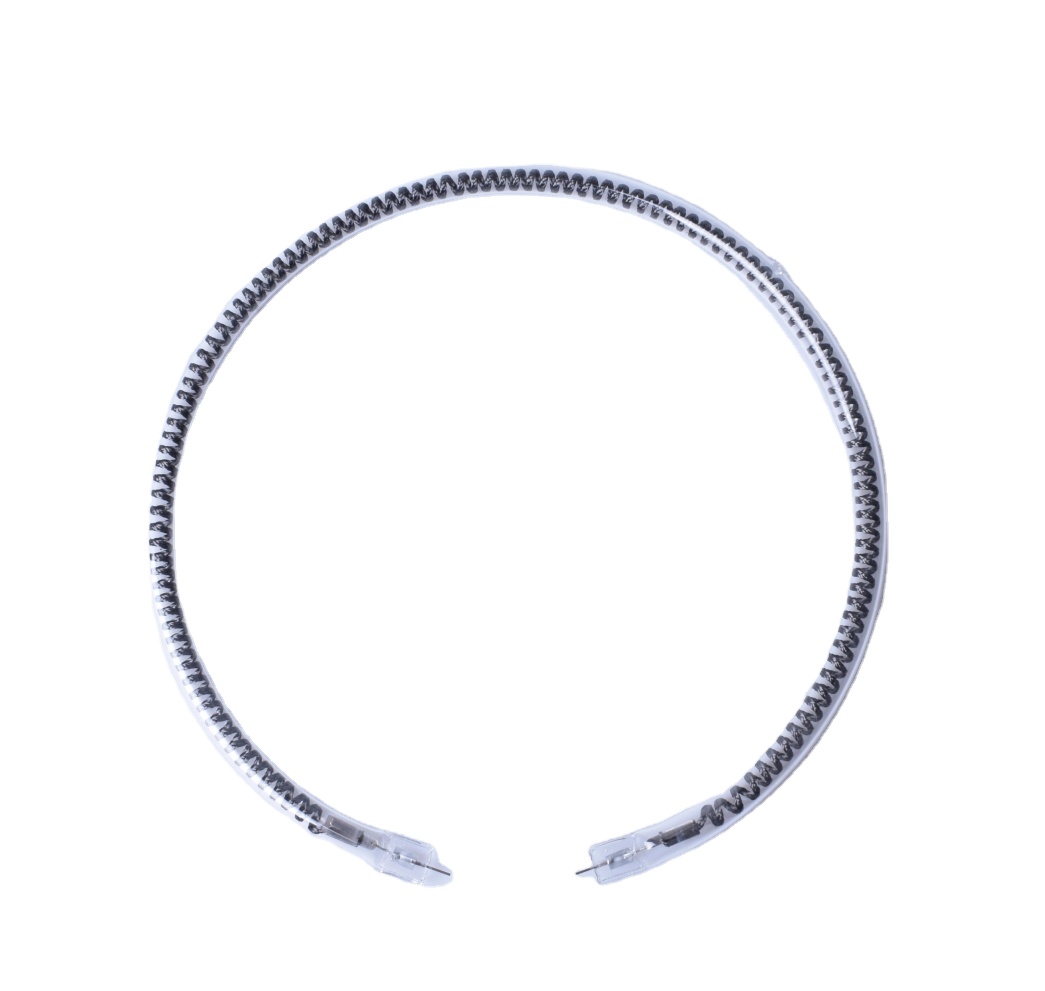
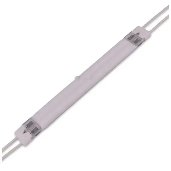
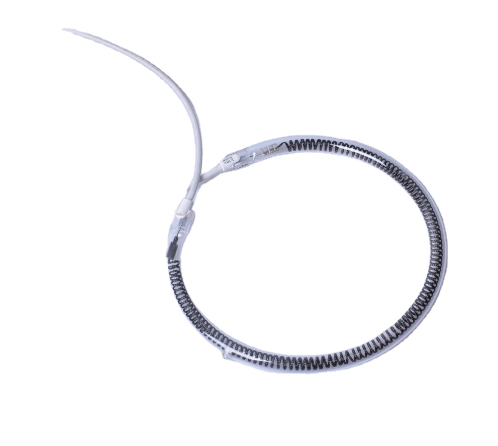
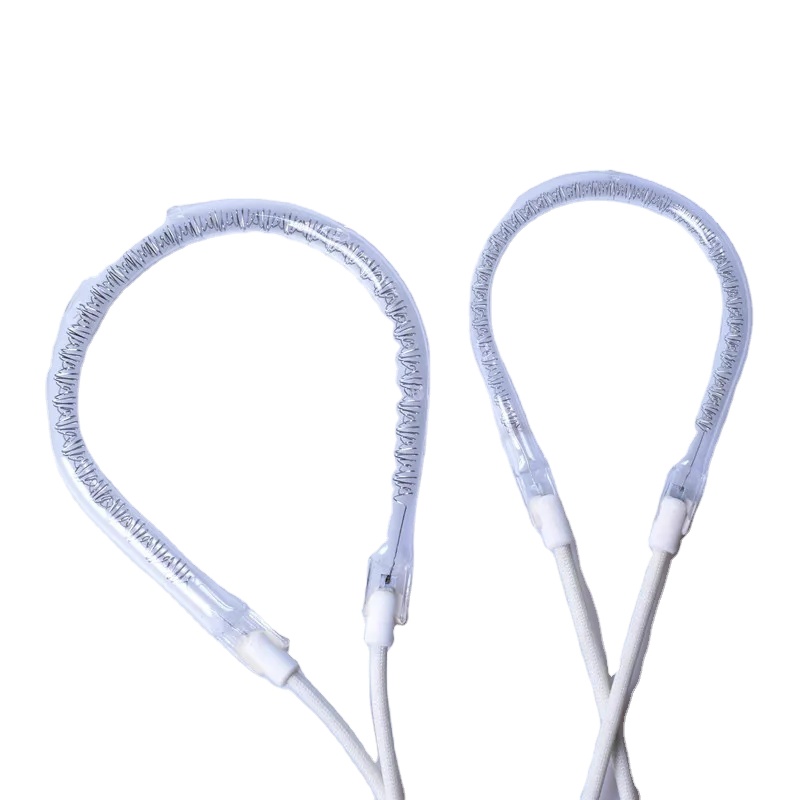
In the Santa Clara Valley microelectronics and clean technology corridor, component thermal shock resistance and chemical non-reactivity are essential parameters. Semiconductor fabrication, additive manufacturing, and optical research laboratories require thermal management parts that do not introduce micro-contaminants or fail during rapid thermal cycling.
Kavri Quartz components are engineered precisely for the San Jose hardware manufacturing and semiconductor tool ecosystem:
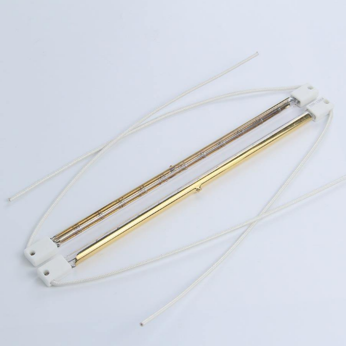
Silicon Valley wafer processing fabs rely on high-flux short-wave tungsten-halogen emitters with sub-second ramp rates. Our precision fused quartz envelopes allow maximum energy throughput across the 0.8–1.4 µm spectrum, providing ultra-clean, uniform thermal gradients that mitigate slip dislocations during rapid annealing.
Our pure synthetic fused silica plates, boats, and tubes operate with high mechanical integrity inside reactive ion etching (RIE) tools and chemical vapor deposition (CVD) chambers. With an exceptionally low coefficient of thermal expansion (5.5 × 10¯&sup7;/K), components maintain strict planar tolerances without outgassing trace alkalis.
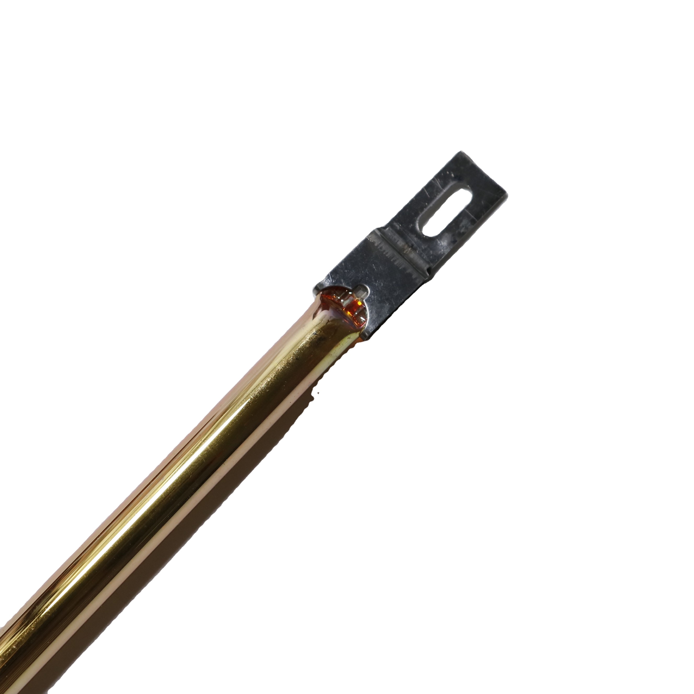
For San Jose’s advanced robotics, photonics, and precision medical device packaging assemblies, our custom UV cure lamps and gold-backed twin-tube emitters deliver exact-dose radiative drying. Backed by custom reflective layers, energy directs straight to structural polymers without raising substrate temperatures.
Engineered to exceed ASTM and CE directives for mission-critical industrial heating and semiconductor vacuum handling.
| Property Matrix | Typical Metric Value | Imperial Equivalent | Silicon Valley Relevance |
|---|---|---|---|
| Purity (SiO2 Content) | ≥ 99.99% | ≥ 99.99% | Prevents metal-ion contamination in sub-micron fabrication |
| Thermal Expansion (0–300 °C) | 5.5 × 10¯&sup7; cm/cm °C | 3.1 × 10¯&sup7; in/in °F | Zero deformation under instant 1000 °C/sec flash cycles |
| Continuous Operating Temp | 1100 °C | 2012 °F | Withstands high-temperature diffusion and furnace firing |
| Softening Point | 1683 °C | 3061 °F | Structural stability in aggressive chamber environments |
| Dielectric Strength (20 °C, 1MHz) | 25–40 kV/mm | 635–1016 V/mil | Superior electrical insulation for high-voltage plasma rigs |
| Spectral Transmission (Transmittance) | > 90% (260nm – 2500nm) | UV through Short/Medium IR | High directional efficiency for radiant lamp bulbs |
The manufacturing landscape across the South Bay and East Bay is undergoing a profound shift. Driven by CHIPS and Science Act investments, electrification initiatives, and localized hardware prototype hubs, procurement engineers in San Jose, Fremont, and Santa Clara are adapting to three primary industry trends:
Traditional convection ovens and legacy batch furnaces consume significant energy and present thermal lag. Silicon Valley clean manufacturing teams are adopting high-density directional IR radiant lamps that transfer heat directly to target substrates via electromagnetic radiation, cutting kilowatt-hour consumption by up to 42%.
As advanced packaging lines expand across Santa Clara County for AI accelerators and photonics, tolerance for hydroxyl (OH-) radicals and metal impurities (Fe, Cu, Ni) has dropped to parts-per-billion levels. Quartz components require tightly controlled electric melting and vacuum dehydroxylation processes.
Silicon Valley hardware teams prioritize cycle velocity. R&D centers require agile batching (10 to 500 units) of custom-curved emitters, twin-bore tubes, and CNC-milled quartz plates without bearing prohibitive non-recurring engineering (NRE) tooling charges or multi-month lead times.
Combining raw mineral extraction advantages with precision craftsmanship to serve demanding global supply chains.
Located in Lianyungang, Jiangsu, adjacent to the Donghai silica basin—one of the world's premier quartz centers. This proximity gives us unhindered access to raw crystal silica materials, reducing procurement overhead while preserving high mineral purity.
Founded in 2014, Kavri Quartz maintains 3 automated fabrication lines producing custom-engineered emitters, twin tubes, and custom glassware. We support bespoke voltages (12V to 480V), tailored wattages, custom lead terminations, and buyer private-labeling.
With an onsite-verified facility and an international trade history where over 85% of volume ships to North America, Europe, and East Asia, our technical team commits to an inquiry response window of ≤ 4 hours, accelerating your validation timelines.
Every lot undergoes stringent dimensional inspection, filament alignment verification, gas seal integrity checks, and coating adhesion tests. We supply full spectral data sheets and material certs for seamless compliance within your ISO/CE framework.
Unlike massive glass conglomerates demanding thousands of units, our baseline order volumes start from 8–10 pieces for standard elements, providing Bay Area incubators and machine builders a path from prototyping to volume manufacturing.
We provide full-spectrum Incoterms (EXW, FOB, CIF, DDP). Utilizing multi-layer, shock-isolated engineered foam packaging and vacuum-sealed nitrogen pouches, precision quartz components arrive safely at your facility without breakage or surface contamination.
Addressing the technical, regulatory, and logistics inquiries raised by Northern California procurement teams.
Whether you require standard 1000W short-wave emitters, specialized twin-tube arrays, or custom fused silica chamber windows for your Silicon Valley facility, our engineering staff is standing by to review your CAD files and technical specifications.
Contact Us